When designing and producing products, PCBs can easily become one of the most expensive components in the entire product, so reducing PCB costs may be one of the main factors proven to be beneficial for reducing overall production costs. The main approach is to reduce PCB costs by reducing PCB size, selecting appropriate components, and introducing appropriate design techniques. That’s why in this article, we will describe the most common PCB cost reduction techniques that you can implement when designing and manufacturing PCBs.
Reduce PCB size
Reducing PCB size is the most common PCB cost reduction technique that can be used to reduce PCB costs. There is another positive result, as the reduction in PCB size also leads to a reduction in product size, which is highly effective for different types of applications. In the past, through hole components were widely used components that directly affected the size of PCBs.
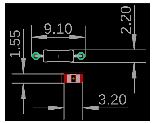
Now, all components can be converted to SMD versions, even ICs, as different manufacturers offer different packaging sizes, which are smaller and can be used to directly reduce PCB size. Please refer to the following figure to understand how the component size significantly reduces the circuit board.

In the above figure, we can see the difference between the through-hole and SMD0805 package size. Now, it is evident that resistors with the same value and power can be used in smaller spaces. You can even place two resistors, one on the top layer and the other on the bottom layer. In addition to 0805, there are also smaller sizes such as 0603, 0402, 0201, etc. This is reflected the same in capacitors, diodes, and inductors. A simple electronic circuit uses the largest resistor and capacitor type components, and even reducing these two components can reduce the board size by at least 30-40%.
Other methods to reduce PCB component size:
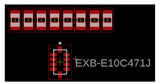
By applying appropriate design and component selection techniques, SMD resistors can even be further reduced, as shown in the resistors below.

8 and 0805 resistors and resistor SIP encapsulation with 8 pins. This is like a chess game where you need to make the right decisions, and reducing PCB size is the right move. SMD components are also relatively cheaper than through hole components, both in terms of component cost and assembly related situations. Okay, once again, there is a reason for this, as the through hole component requires additional steps to cut the component leads and weld them to the board.
Reduce unnecessary layers and poor layer specifications
Almost always, people have added unnecessary layers for different reasons (such as thermal compensation), poor routing experience, and so on. If the number of layers is reduced from 6 to 4, from 4 to 2, etc., it can save a lot of money in the manufacturing process of circuit boards. One of the important things to remember is the method of minimizing the number of circuit board layers as much as possible. However, for complex circuit boards containing spherical packaging or extensive wiring, a higher number of layers is necessary for better signal quality and overall circuit board performance. In this case, the increased cost can better save additional rework costs, so it is important to correctly determine how many layers should be used for circuit board design.
Another common mistake made by designers is to provide incorrect layer specifications to suppliers, resulting in high PCB costs during the production process. Does your design require a copper thickness of 70 microns for all layers? Can 17.50 micron circuit boards be made on the top and bottom layers, as well as 35 microns on the inner layer, and vice versa? There will be a significant cost reduction during the production process. In addition, please specify an appropriate creepage distance for your PCB.
Circuit board material:
By selecting appropriate sheet materials, costs can be reduced. In many cases and in many different applications, the standard FR-4 board is everything that can be done, and choosing a more expensive option does not have any impact, making it a luxury item. The temperature level can be the standard 130-140 degrees, and can be used in any situation unless there are special requirements.
PCB thickness:
The cost of non-standard PCB thickness increases. 1.6mm is the standard PCB thickness. Increasing or reducing PCB thickness will attract more funds for the production phase.
Solder resistance layer and legend color:
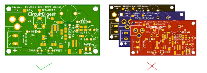
In addition, try to use a green solder mask layer instead of creating fancy colored PCBs such as black, red, and blue. These are a wide range of color choices and will incur significant costs in PCB manufacturing. The green solder mask layer is widely used in the PCB manufacturing process and is the cheapest choice for PCBs. This rule also applies to legend colors. The most common legend color is white. Choosing other colors such as black will greatly increase PCB production costs. This theory applies to most manufacturers, but some manufacturers charge the same price for all different solder mask layers and screen printing options.

Surface treatment:
Using heavy metal/ENIG for unnecessary reasons is a bad choice and incurs PCB costs. High speed, impedance controlled wiring requires correct locking of signal integrity. Do you need to complete this operation on any simple board? Tin immersion or HAL (Sn Pb) can be used to reduce production costs.
Routing related compensation
Adding buried and blind holes in the PCB manufacturing process can incur significant costs. Change the design in a way that allows for wiring without the need for buried or blind holes. In addition, sometimes, in order to make wiring easier, people place components in a certain order and are forced to manually weld the components during the assembly process. This is not a cost-effective choice.
Believe me, in almost all cases, good design practice can reduce the chance of using buried or blind holes until it is a truly dense circuit board that requires signal integrity where buried or blind holes are needed.
Adjust order quantity and delivery time
The last but not least important component, assembly, or manufacturing of PCBs, with order volume being the main factor in reducing production costs. It is inversely proportional to the price. Generally speaking, as the order volume increases, the manufacturing cost of PCBs will decrease. You can plan and adjust the order quantity based on the selected PCB manufacturer to meet your order quantity. Always compare the price of the required PC with the quantity required in the future. However, please ensure that the circuit board is well tested during the POC (Proof of Concept) phase and the design is finalized for production. Placing an order without testing a PCB is a waste of time and involves a lot of money.
Now, you need to know the delivery time. Order a PCB when you are not in a hurry and set a perfect goal before starting the production project, providing compensation related to time. Different suppliers have different delivery time related rules. If you order a PCB with a very short delivery time, the cost of the PCB will become very high. Therefore, please always adjust the delivery time to obtain the lowest cost quotation on the PCB. For mass production, saving a few dollars may not be much for a single circuit board, but it may have a huge impact on larger batch production.


