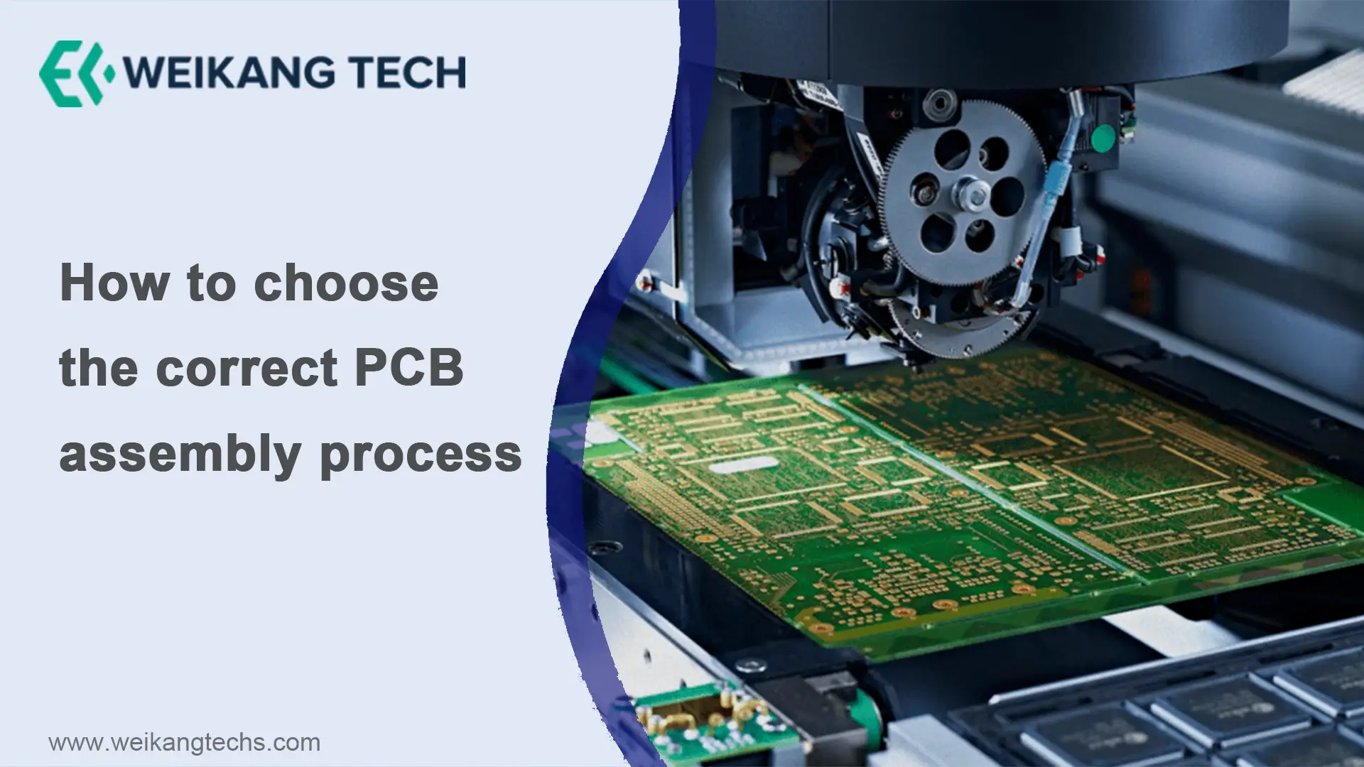
Choosing the correct PCB assembly process is crucial as this decision directly affects the efficiency and cost of the manufacturing process, as well as the quality and performance of the application.
PCB assembly is usually carried out using one of the following two methods: surface mounting technology or through hole manufacturing. Surface mount technology is the most widely used PCB component. Through-hole manufacturing is less commonly used, but it is still very popular, especially in certain industries.
The process of choosing a PCB assembly process depends on many factors. To help you make the right choice, we have compiled this brief guide to choose the correct PCB assembly process.
PCB assembly: surface mount technology
Surface mount technology is the most commonly used PCB assembly process. It is used in many electronic products, from USB flash drives and smartphones to medical devices and portable navigation systems.
- This PCB assembly process allows for the manufacturing of smaller and smaller products. If space is very valuable, then if your design has components such as resistors and diodes, then this is your best choice.
- Surface mount technology can achieve a higher degree of automation, which means that circuit boards can be assembled at a faster speed. Compared to the placement of through-hole components, this enables you to process PCBs in large quantities and has higher cost-effectiveness.
- If you have unique requirements, surface mount technology may be highly customizable and therefore the right choice. If you need a custom designed PCB, this process is flexible and powerful, providing the desired results.
By using surface mount technology, components can be fixed on both sides of the circuit board. This dual sided circuit board feature means that you can apply more complex circuits without expanding the application range.
PCB assembly: through-hole manufacturing
Although the use of through-hole manufacturing is decreasing, it is still a common PCB assembly process.
PCB components manufactured using through holes are used for large components such as transformers, semiconductors, and electrolytic capacitors, providing a stronger bond between circuit boards and applications.
As a result, through-hole manufacturing provides a higher level of durability and reliability. This additional security makes this process the preferred option for applications used in sectors such as aerospace and military industry.
- If your application must withstand high levels of pressure (whether mechanical or environmental) during operation, the best choice for PCB assembly is through hole manufacturing.
- If your application must run at high speed and at the highest level under these conditions, then through-hole manufacturing may be a suitable process for you.
- If your application must run at high and low temperatures, the higher strength, durability, and reliability of through-hole manufacturing may be your best choice.
- If it is necessary to operate under high pressure conditions and maintain its performance, through-hole manufacturing may be the most suitable PCB assembly process for your application.
In addition, due to continuous innovation and growing demand for increasingly complex electronic products, these electronic products require increasingly complex, integrated, and smaller PCBs, so your application may require two types of PCB assembly technology. This process is called “hybrid technology”.
Determine your PCB assembly process
This guide provides quick insight into which PCB assembly process is most suitable for your application. However, there may be other factors that make decision-making more complex.


